____________________ > Aurora
> System components
> Old Style
> Hydrolic Components
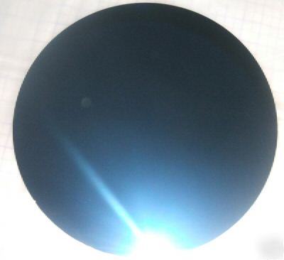
> 12 inch hafnium oxide high k wafer
12 inch hafnium oxide high k wafer
You are looking on a 300mm Blanket Hafnium Oxide High K Wafer.
The fundamental building blocks for all computer chips transistors have tracked with Moore's Law for forty years. Intel has led the industry in transistor gate dielectric scaling using silicon dioxide (SiO2) for seven logic-process generations over the last 15 years. But as transistors shrink, leakage current can increase. Managing that leakage is crucial for reliable high-speed operation, and is becoming an increasingly important factor in chip design. Major semiconductor companies have made a significant breakthrough in solving the chip power problem, identifying a new "high-k" (high dielectric constant) material called hafnium dioxide to replace the transistor's silicon dioxide gate dielectric, and new metals to replace the polysilicon gate electrode of NMOS and PMOS transistors. These new materials, along with the right process recipe, reduce gate leakage more than 100-fold, while delivering record transistor performance.
Hafnium Dioxide (HfO2) is novel high dielectric constant material of semiconductor industry for sub-45nm node microchip manufacturing technology.
A CVD Hafnium Dioxide layer has been deposited on the single crystal silicon wafer. The thickness of HfO2 is not sure.
The wafer looks like new and is well packaged so that you could use it as research too.
You should keep the wafer in a clean, dry condition to avoid the surface pollution and scratching.
The Wafer is very fragile, a broken wafer can be dangerous due to the sharp edges can cause injuries. Consider it as thin glassware, handle and display it with care. Keep away to the children. We will pack it very well for transport.