____________________ > Auburn
> System components
> New Style
> Tools
> Power tools
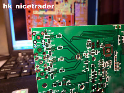
> Double layer pcb etching prototype fabrication
Double layer pcb etching prototype fabrication
*** Double Layer PCB Etching Prototype Fabrication ***
Files Types: Gerber 274-X, 274 and Aperture file
Maximum Panel Size: 500mm x 1100mm
Board Size Tolerance: +/- 0.2mm
Board Thickness: 0.4mm - 2.4mm
Board Thickless Tolerance: +/- 10%
Minimum Line Width and Spacing: 0.1524mm
Surface Finish: Immersion Gold / Electrolytic Gold / HASL(Sn/Pb) / HASL Lead free
Standard Lead Time: 5 - 7 business days
1. Send the gerber files, fabrication drawings, desired quantities and other demand to ****@yahoo.com.hk
We promise FREE to re-fab any fault PCB!